Microelectronics Research Development Corporation
Technology
Overview
Radiation Hardening By Design (RHBD) is a methodology based on a set of electrical and layout design techniques that mitigate the effects of nuclear and natural space radiation on microcircuits. A number of RHBD techniques are used to meet the hardening goals and requirements of Micro-RDC's integrated circuits. These goals include:
Micro-RDC is well versed in the area of RHBD including development of Application-Specific-Integrated-Circuits (ASIC), general purpose electronic integrated circuits, various radiation-hardened integrated circuits implementing metal oxide semiconductor field effect transistors and electronic circuit board component parts providing radiation hardening for digital logic architectures. We have in the past contributed heavily to the DARPA RHBD research and development program under subcontract to Boeing. Our earlier work was in bulk CMOS technologies in which we developed cell libraries that were hardened to Total Ionizing Dose (TID) to > 1 MRad(Si) using a variety of specialized layout techniques to address the TID effects of transistor edge leakage and field oxide leakage as well as single event induced latchup.
Presentations/Publications
Overview
Radiation Hardening By Design (RHBD) is a methodology based on a set of electrical and layout design techniques that mitigate the effects of nuclear and natural space radiation on microcircuits. A number of RHBD techniques are used to meet the hardening goals and requirements of Micro-RDC's integrated circuits. These goals include:
- Latchup: None
- Total Ionizing Dose: > 1 MRad(Si)
- Soft Error Rate: < 1 x 10⁻¹⁰ Errors/Bit-Day
- Transient Dose Rate
- Upset: > 1 x 10¹⁰ Rad(Si)/s
- Survivability: > 1 x 10¹² Rad(Si)/s
Micro-RDC is well versed in the area of RHBD including development of Application-Specific-Integrated-Circuits (ASIC), general purpose electronic integrated circuits, various radiation-hardened integrated circuits implementing metal oxide semiconductor field effect transistors and electronic circuit board component parts providing radiation hardening for digital logic architectures. We have in the past contributed heavily to the DARPA RHBD research and development program under subcontract to Boeing. Our earlier work was in bulk CMOS technologies in which we developed cell libraries that were hardened to Total Ionizing Dose (TID) to > 1 MRad(Si) using a variety of specialized layout techniques to address the TID effects of transistor edge leakage and field oxide leakage as well as single event induced latchup.
Presentations/Publications
High Density Packaging
The High Density Interconnect (HDI) process allows for complex designs to be packaged for spaceborne applications meeting the demands for high density logic; speed, low power and small size and weight while accommodating high pin counts. In addition, with the BGA HDI solutions, we meet the requirements for reliability and survival in the harsh environments encountered in spaceborne applications including ultra high acceleration and temperature cycling.
Single Event Effects
Micro-RDC predominately uses circuit techniques to mitigate the SEE effects of Single Event Upset (SEU) and Single Event Transient (SET) induced upset. Temporal sampling techniques are used to harden data latches. Conventional 6-transistor SRAM cells, with a moderate amount of capacitive hardening (to increase the threshold above direct proton upset), are used for on-chip dual port SRAM. More exotic 8- and 12-transistor SRAM cells have proven to be an ineffective hardening alternative in deep submicron technologies since critical nodes cannot be sufficiently separated to prevent a simultaneous strike by a single heavy ion incident at a high angle. Additional parity bits are provided for each data word and SEU hardness is achieved by large bit separations along with Error Detection And Correction (EDAC) techniques. Memory scrubbing algorithms, usually required for devices operating in high fluency proton environments, can also be implemented.
Data SEU and SET induced data errors in sequential logic cells have become the principal problems precluding the use of deep submicron technologies in both space and nuclear environments. As feature sizes shrink and power supply voltages are reduced, the critical charge threshold for upset is reduced as the square of the feature size. Furthermore, the abundance of particles with LET large enough to generate the critical charge goes up by 2 to 4 orders of magnitude. The higher energy particles produce the low LET strikes, and the earth's magnetic field is less effective in screening high-energy particles. Consequently, even LEO satellites will have increasing problems with SEU/SET as they employ deep submicron technologies.
Furthermore, reducing feature size is making the switching speeds much faster, decreasing the propagation delay in logic cells, and increasing the clock frequency. As a result, SETs generated in combinatorial logic will propagate freely and be indistinguishable from normal circuit signals. Furthermore, the probability that SET errors will be latched into registers is increasing proportionally to the clock frequency.
Recent characterizations of the IBM SOI technologies have shown that SET pulse widths are much smaller (<100 ps) than previously measured in bulk technologies (~1 ns). Thus our choice of the IBM 45 nm SOI simplifies our hardening to SETs.
It should be noted that Triple Modular Redundancy (TMR) or DICE-based latches only help prevent static SEU and do nothing to prevent SET induced data errors. Also, TMR or DICE hardening is susceptible to static SEU if an incident heavy ion travels through the silicon just under the IC surface and strikes more than one critical node.
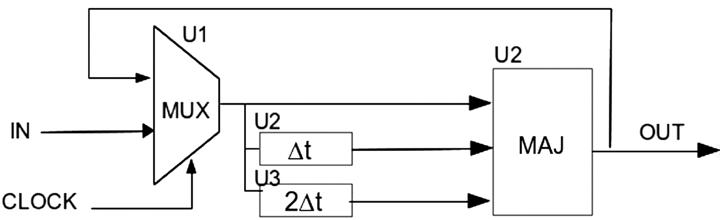
We therefore use our temporal sampling latch methodology as illustrated below. This illustrates our approach for a level sensitive latch. A standard D-Flip-Flop is built from two such latches coupled in a master-slave configuration.
An unhardened latch is nothing more than a 2-input MUX (multiplexer) with its output fed back to one of its inputs and the select line controlled by the clock signal. For the temporal filtering version shown above, the MUX (U1) output is time sampled using a voting circuit (U2) at three separate times as determined by the sampling delay elements (U3 and U4). Only the majority of the sampling is fed back to the MUX. By using the single MUX at three separate times, we effectively replicate it, not in space, but in time and achieve the equivalent of triple spatial redundancy without the area penalty. More importantly, however, the latch is immune to SET induced errors on any node (data input, clock input, or any node internal to the latch) provided that the sampling delay (deltaT) is longer than the SET pulse width. Also, by increasing the delay deltaT to exceed the SET width pulse plus the loop delay (U1+U2), the latch can be made immune to upset from multiple node strikes. Since the transient widths increase with increasing LET, variable delays are often used for the elements U3 and U4 so that one can simply "dial up" the desired level of immunity based on the fielded environment.
A mixed-signal block, such as a PLL or a SERDES, can also be sensitive to SETs which can cause adverse voltage amplitude and phase changes. For such circuitry we use a new and proprietary hardening approach recently developed at Micro-RDC. This approach employs new Multiple Interlocked CEll (MICETM) circuits which mitigate both static latch SEU as well as SET induced errors in both sequential and combinatorial logic circuits. In its most robust form, MICE provides immunity to multiple critical node, as well as to single critical node, heavy-ion strikes.
Key features of MICE include circuits having multiple isolated nodes which, during a heavy-ion strike, will not switch to an incorrect state, but will only switch to a HI-Z state. Immunity to heavy-ion effects is then achieved in this architecture by:
1. Isolating any struck node to prevent the error from propagating through the circuit, and
2. Providing a means to recover the correct logic state in any circuit connected to the upset node through the redundant data paths.
It is then the multiple interlocked nature of MICE logic that provides the necessary hardness without incurring the speed penalties associated with SET filtering.
Dose rate hardness, while a major issue in nuclear radiation environments, is a much lesser concern in the natural space environments typically encountered in science missions. The IBM SOI technology, because of the small collection volumes associated with the thin (~50 nm) silicon layer over the buried oxide, automatically provides inherent dose rate upset hardness and survivability without the need for any additional design hardening considerations.
Total immunity to latchup is the only acceptable hardness level for radiation environments. In earlier bulk technologies, the preferred RHBD approach to eliminate latchup was to use guard rings and to actively control substrate and well voltages (the base regions of the parasitic bipolar devices responsible for latchup) through the prolific use of substrate and well contacts. In SOI technologies active regions are dielectrically isolated from one another and latch paths no longer exist. One must still, however, consider the possibility of snap back, particularly in the NMOS transistor devices operating at the higher voltages in the IO blocks.
The High Density Interconnect (HDI) process allows for complex designs to be packaged for spaceborne applications meeting the demands for high density logic; speed, low power and small size and weight while accommodating high pin counts. In addition, with the BGA HDI solutions, we meet the requirements for reliability and survival in the harsh environments encountered in spaceborne applications including ultra high acceleration and temperature cycling.
Single Event Effects
Micro-RDC predominately uses circuit techniques to mitigate the SEE effects of Single Event Upset (SEU) and Single Event Transient (SET) induced upset. Temporal sampling techniques are used to harden data latches. Conventional 6-transistor SRAM cells, with a moderate amount of capacitive hardening (to increase the threshold above direct proton upset), are used for on-chip dual port SRAM. More exotic 8- and 12-transistor SRAM cells have proven to be an ineffective hardening alternative in deep submicron technologies since critical nodes cannot be sufficiently separated to prevent a simultaneous strike by a single heavy ion incident at a high angle. Additional parity bits are provided for each data word and SEU hardness is achieved by large bit separations along with Error Detection And Correction (EDAC) techniques. Memory scrubbing algorithms, usually required for devices operating in high fluency proton environments, can also be implemented.
Data SEU and SET induced data errors in sequential logic cells have become the principal problems precluding the use of deep submicron technologies in both space and nuclear environments. As feature sizes shrink and power supply voltages are reduced, the critical charge threshold for upset is reduced as the square of the feature size. Furthermore, the abundance of particles with LET large enough to generate the critical charge goes up by 2 to 4 orders of magnitude. The higher energy particles produce the low LET strikes, and the earth's magnetic field is less effective in screening high-energy particles. Consequently, even LEO satellites will have increasing problems with SEU/SET as they employ deep submicron technologies.
Furthermore, reducing feature size is making the switching speeds much faster, decreasing the propagation delay in logic cells, and increasing the clock frequency. As a result, SETs generated in combinatorial logic will propagate freely and be indistinguishable from normal circuit signals. Furthermore, the probability that SET errors will be latched into registers is increasing proportionally to the clock frequency.
Recent characterizations of the IBM SOI technologies have shown that SET pulse widths are much smaller (<100 ps) than previously measured in bulk technologies (~1 ns). Thus our choice of the IBM 45 nm SOI simplifies our hardening to SETs.
It should be noted that Triple Modular Redundancy (TMR) or DICE-based latches only help prevent static SEU and do nothing to prevent SET induced data errors. Also, TMR or DICE hardening is susceptible to static SEU if an incident heavy ion travels through the silicon just under the IC surface and strikes more than one critical node.
We therefore use our temporal sampling latch methodology as illustrated below. This illustrates our approach for a level sensitive latch. A standard D-Flip-Flop is built from two such latches coupled in a master-slave configuration.
An unhardened latch is nothing more than a 2-input MUX (multiplexer) with its output fed back to one of its inputs and the select line controlled by the clock signal. For the temporal filtering version shown above, the MUX (U1) output is time sampled using a voting circuit (U2) at three separate times as determined by the sampling delay elements (U3 and U4). Only the majority of the sampling is fed back to the MUX. By using the single MUX at three separate times, we effectively replicate it, not in space, but in time and achieve the equivalent of triple spatial redundancy without the area penalty. More importantly, however, the latch is immune to SET induced errors on any node (data input, clock input, or any node internal to the latch) provided that the sampling delay (deltaT) is longer than the SET pulse width. Also, by increasing the delay deltaT to exceed the SET width pulse plus the loop delay (U1+U2), the latch can be made immune to upset from multiple node strikes. Since the transient widths increase with increasing LET, variable delays are often used for the elements U3 and U4 so that one can simply "dial up" the desired level of immunity based on the fielded environment.
A mixed-signal block, such as a PLL or a SERDES, can also be sensitive to SETs which can cause adverse voltage amplitude and phase changes. For such circuitry we use a new and proprietary hardening approach recently developed at Micro-RDC. This approach employs new Multiple Interlocked CEll (MICETM) circuits which mitigate both static latch SEU as well as SET induced errors in both sequential and combinatorial logic circuits. In its most robust form, MICE provides immunity to multiple critical node, as well as to single critical node, heavy-ion strikes.
Key features of MICE include circuits having multiple isolated nodes which, during a heavy-ion strike, will not switch to an incorrect state, but will only switch to a HI-Z state. Immunity to heavy-ion effects is then achieved in this architecture by:
1. Isolating any struck node to prevent the error from propagating through the circuit, and
2. Providing a means to recover the correct logic state in any circuit connected to the upset node through the redundant data paths.
It is then the multiple interlocked nature of MICE logic that provides the necessary hardness without incurring the speed penalties associated with SET filtering.
Dose rate hardness, while a major issue in nuclear radiation environments, is a much lesser concern in the natural space environments typically encountered in science missions. The IBM SOI technology, because of the small collection volumes associated with the thin (~50 nm) silicon layer over the buried oxide, automatically provides inherent dose rate upset hardness and survivability without the need for any additional design hardening considerations.
Total immunity to latchup is the only acceptable hardness level for radiation environments. In earlier bulk technologies, the preferred RHBD approach to eliminate latchup was to use guard rings and to actively control substrate and well voltages (the base regions of the parasitic bipolar devices responsible for latchup) through the prolific use of substrate and well contacts. In SOI technologies active regions are dielectrically isolated from one another and latch paths no longer exist. One must still, however, consider the possibility of snap back, particularly in the NMOS transistor devices operating at the higher voltages in the IO blocks.
Temporal Sampling Latch
Copyright 2022 Microelectronics Research Development Corporation. All Rights Reserved.
